Copper Stamping, Copper Stamped Parts, and Copper Stamped Components – Precision Manufacturing Solutions
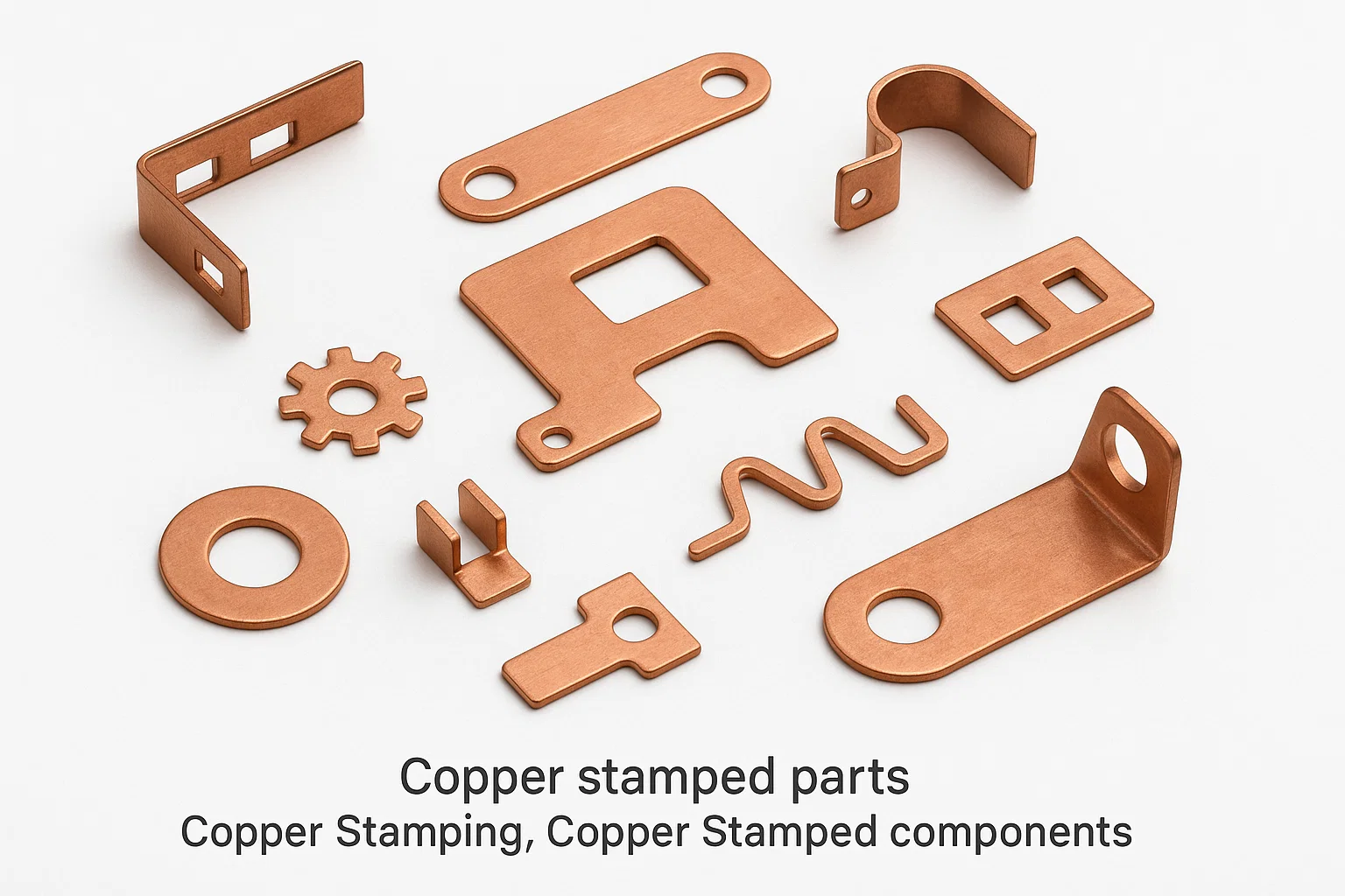
We are one of the leading manufacturers and exporters of Copper Stamping, Copper Stamped Parts, and Copper Stamped Components from India. We have been supplying precision-engineered Copper pressed parts, Copper terminals, Copper lugs, and custom Copper stamped components to the world market for many decades. Our state-of-the-art manufacturing facility combines traditional expertise with modern progressive die stamping technology to deliver superior quality Copper press work that meets the most demanding specifications across electrical, automotive, telecommunications, and industrial sectors. With over three decades of global exposure, our engineering team brings unparalleled technical knowledge to every project, from simple Copper pressed clips to complex multi-stage Copper stamped terminals. Our commitment to precision tolerances, competitive pricing, and exceptional customer service has established us as a trusted Copper stamping supplier to Fortune 500 companies and innovative startups alike across North America, Europe, Australia, and Asia-Pacific regions.
Price: US$ 14.30/Kilogram CIF US Sea port
Comprehensive Overview of Copper Stamping Services
Copper stamping represents a fundamental metal forming process that transforms flat Copper sheets into three-dimensional functional components through the application of controlled force using precision dies and punch presses. This cold working manufacturing method leverages the exceptional ductility and malleability of Copper alloys to create intricate geometries, tight tolerances, and consistent repeatability across production volumes ranging from prototype quantities to millions of pieces annually. Our advanced Copper stamping capabilities encompass blanking, piercing, forming, bending, coining, embossing, and progressive die operations that deliver cost-effective solutions for electrical connectors, terminals, contacts, busbars, heat sinks, shielding components, brackets, clips, clamps, and specialized switching elements.
The technical advantages of Copper stamping over alternative manufacturing processes include minimal material waste, rapid production cycles, excellent dimensional consistency, superior surface finish quality, and the ability to integrate multiple forming operations within a single progressive die sequence. Our engineering team utilizes Computer-Aided Design (CAD) and Computer-Aided Manufacturing (CAM) software to optimize die layouts, predict material flow characteristics, minimize springback effects, and ensure first-time-right tooling development. Material utilization efficiency typically exceeds 85 percent through strategic nesting algorithms and scrap reduction techniques, translating to significant cost savings for high-volume production runs.
Copper’s inherent properties including exceptional electrical conductivity (approximately 100 percent IACS for pure Copper), excellent thermal conductivity (around 391 W/m·K), superior corrosion resistance, antimicrobial characteristics, and outstanding formability make it the material of choice for critical applications in power distribution systems, electronic devices, telecommunications infrastructure, renewable energy installations, and transportation electrification. Our Copper stamping operations maintain rigorous quality control protocols throughout the manufacturing cycle, from incoming material inspection and first article verification to in-process dimensional checks and final statistical process control documentation.
Copper Stamping
Copper stamping encompasses the complete spectrum of sheet metal fabrication techniques specifically optimized for Copper and Copper alloy materials. This precision manufacturing process involves positioning Copper strip or sheet material between specially designed tooling sets, then applying tremendous force through mechanical or hydraulic press systems to shear, form, or deform the material into the desired configuration. The stamping operation can be executed as a single-stage process for simple geometries or as a multi-station progressive die sequence for complex components requiring multiple forming operations. Our Copper stamping capabilities extend from 0.1 millimeter ultra-thin foils used in flexible printed circuit board applications to 6 millimeter heavy-gauge plates for industrial busbar systems and power distribution components. The process parameters including press tonnage, stroke speed, material feed rate, die clearances, and lubrication systems are meticulously calibrated to accommodate the specific work-hardening characteristics and annealing requirements of different Copper grades. Advanced sensors and monitoring systems track press force signatures, material positioning accuracy, and part ejection cycles to maintain consistent quality throughout extended production runs. Our investment in servo-driven press technology enables precise control over ram velocity profiles, dwell times at bottom dead center, and gentle part ejection sequences that minimize deformation and surface marking on delicate Copper components.
Copper Stamped Parts
Copper stamped parts represent the finished components produced through various stamping operations, encompassing an extensive range of functional elements used across diverse industrial applications. These precision-manufactured parts include electrical terminals, connector housings, contact springs, grounding straps, shielding cans, heat dissipation fins, mounting brackets, wire retention clips, fuse elements, switch contacts, relay components, transformer laminations, motor commutator segments, printed circuit board tabs, battery terminals, automotive electrical components, and specialized fastening hardware. Each Copper stamped part undergoes rigorous dimensional verification using coordinate measuring machines (CMM), optical comparators, and specialized gauging fixtures to ensure compliance with customer specifications and industry standards. Our quality assurance protocols include material certification traceability, hardness testing using Rockwell or Vickers methods, electrical conductivity verification, surface finish analysis, and functional performance validation under simulated operating conditions. The production flexibility of our manufacturing systems allows seamless transitions between different part geometries, accommodating both high-volume standardized components and low-volume custom-designed parts within the same production schedule. Post-stamping secondary operations available at our facility include deburring through vibratory finishing or barrel tumbling, heat treatment for stress relief or property modification, precision machining for critical features requiring tighter tolerances than achievable through stamping alone, and assembly operations including riveting, welding, or mechanical fastening of multiple stamped components into functional subassemblies.
Copper Stamped Components
Copper stamped components specifically refer to engineered assemblies and subassemblies that incorporate one or more Copper stamped parts into functional units ready for integration into end-use products. These components often combine Copper stamped elements with insulating materials, protective coatings, threaded inserts, or complementary metal components to create complete solutions for electrical connectivity, thermal management, electromagnetic shielding, or mechanical fastening applications. Our component engineering capabilities include design for manufacturability (DFM) consultation where our technical team collaborates with customers to optimize part geometry for stamping efficiency, material selection guidance based on performance requirements and cost considerations, tolerance stack-up analysis to ensure proper fit and function in assemblies, and prototype development using soft tooling or additive manufacturing for functional validation before committing to production tooling investment. The integration of value-added processes such as selective plating application, overmolding with engineering thermoplastics, laser marking for part identification and traceability, and precision assembly under controlled environmental conditions distinguishes our Copper stamped components from commodity parts. Statistical process control charting, failure mode and effects analysis (FMEA), and production part approval process (PPAP) documentation provide customers with confidence in the reliability and consistency of components sourced from our facility.
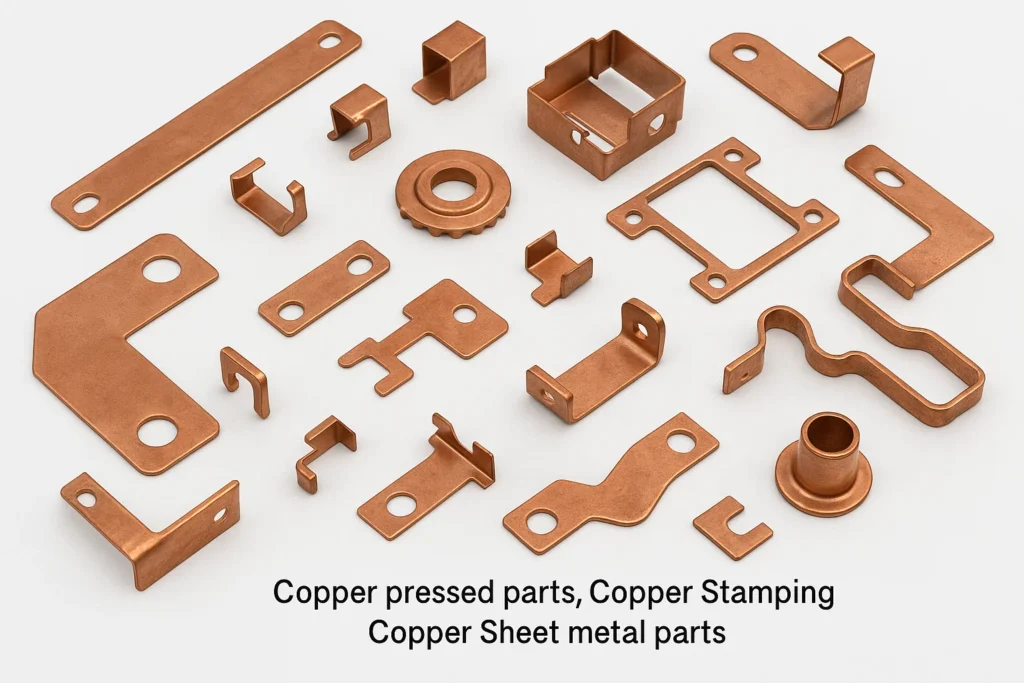
Copper Pressed Parts
Copper pressed parts are manufactured through dedicated pressing operations that emphasize forming, bending, and shaping processes rather than cutting or piercing operations. These parts typically feature deep-drawn geometries, complex three-dimensional contours, coined surfaces with fine detail reproduction, or embossed features that require controlled metal flow under high compressive forces. The pressing process for Copper materials demands careful attention to work hardening phenomena, where the material strength increases but ductility decreases during plastic deformation. Our process engineers strategically incorporate intermediate annealing cycles for deep-drawn Copper parts requiring multiple forming stages, preventing crack formation and ensuring uniform wall thickness distribution throughout the component. Copper pressed parts manufactured at our facility include electrical enclosures with seamless construction, heat exchanger fins with optimized surface area configurations, decorative architectural elements, jewelry components, musical instrument parts, and specialized industrial fittings. The tooling design for Copper pressing operations incorporates generous radii at bend locations to prevent material thinning and cracking, draw beads or blankholder systems to control material flow and prevent wrinkling, and ejector mechanisms that minimize surface contact and marking on finished components. Hydraulic presses with programmable pressure profiles enable precise control over forming forces throughout the pressing cycle, while quick-change tooling systems minimize setup times and maximize equipment utilization across diverse part families.
Copper Pressed Components
Copper pressed components encompass finished assemblies that leverage the unique capabilities of press forming to create functional units with superior structural integrity and aesthetic appeal. These components often feature seamless construction without mechanical joints or fasteners, reducing potential failure points and improving reliability in demanding applications. Manufacturing processes for Copper pressed components include hydroforming where pressurized fluid forms the Copper sheet against a die cavity, spin forming for axially symmetric parts like electrical enclosures or lighting reflectors, and rubber pad forming for low-volume production of complex contours without expensive matched metal dies. Our facility capabilities extend to creating Copper pressed components with integrated stiffening ribs, mounting bosses, alignment features, and snap-fit attachment mechanisms formed directly into the component geometry. The elimination of secondary assembly operations reduces manufacturing costs and lead times while improving dimensional accuracy and part-to-part consistency. Applications for Copper pressed components span architectural facades and roofing systems exploiting Copper’s natural weathering patina development, decorative lighting fixtures leveraging Copper’s aesthetic warmth and reflectivity, heat exchanger assemblies requiring optimized thermal transfer surface geometries, and electrical equipment housings providing electromagnetic shielding combined with corrosion resistance.
Copper Press Work
Copper press work represents the comprehensive category of manufacturing operations performed using press equipment to transform Copper raw materials into functional components. This broad classification includes blanking operations that cut component outlines from Copper strip or sheet, punching operations that create holes and apertures, notching that removes material from component edges, lancing that creates tabs or vents without removing material, forming operations that create three-dimensional contours, bending that produces angular features, coining that impresses fine surface details, and embossing that creates raised or recessed patterns. Our press work capabilities span mechanical press systems ranging from 20-ton capacity for delicate electronic components to 400-ton capacity for heavy industrial parts, hydraulic presses providing variable force profiles and extended dwell times for deep drawing operations, and specialized presses including knuckle-joint designs for coining high-precision features and transfer presses for sequential operations on large components exceeding progressive die bed dimensions. The versatility of Copper press work enables economical production across a wide volume spectrum, from prototype quantities using simple single-station tooling to multi-million piece production runs utilizing sophisticated progressive dies with automatic material feeding, in-die sensing, and integrated quality verification systems. Environmental controls within our press department including temperature and humidity regulation ensure consistent material properties and forming behavior throughout seasonal variations, while advanced lubrication systems extend die life and maintain surface finish quality.
Copper Stamped Terminals
Copper stamped terminals constitute critical electrical connection components designed to provide reliable current paths between conductors, printed circuit boards, wire harnesses, and electrical equipment. These precision-engineered terminals feature specific geometric configurations optimized for mechanical retention force, contact resistance minimization, current carrying capacity, and ease of assembly in automated or manual processes. Our manufacturing expertise encompasses ring terminals with crimp barrels and circular mounting holes, spade terminals with forked contact geometries, blade terminals for push-on connections, pin terminals for insertion into sockets or connectors, tab terminals for welded or soldered attachments, and specialized terminals custom-designed for unique application requirements. The stamping process for Copper terminals incorporates tight dimensional controls on critical features including contact surface flatness within 0.025 millimeters, barrel inner diameter tolerances of ±0.05 millimeters for proper wire crimp retention, and hole position accuracy within ±0.1 millimeters for precise mounting alignment. Material selection for terminal applications considers electrical conductivity requirements, mechanical strength for insertion and extraction cycles, resistance to stress relaxation under sustained contact pressure, and compatibility with plating processes for corrosion protection and contact resistance stability. Our terminal production includes integrated quality testing procedures including pull force verification to ensure adequate crimp retention, contact resistance measurement to validate electrical performance, and cross-sectional analysis for crimp quality assessment on representative samples from each production batch.
Copper Stamped Lugs
Copper stamped lugs are heavy-duty electrical connection components engineered for high-current applications in power distribution systems, industrial equipment, transportation electrification, and renewable energy installations. These robust components feature barrel sections designed to accommodate large-diameter conductors through mechanical crimping or compression connections, and terminal sections with mounting holes for bolted attachment to busbars, switchgear, circuit breakers, or equipment terminals. Our Copper lug manufacturing capabilities span compact designs for control circuit applications carrying a few amperes to massive lugs for substation equipment handling thousands of amperes continuously. The stamping process for heavy-gauge Copper lugs requires substantial press capacity, precision die alignment to prevent material cracking during forming operations, and specialized coining operations to achieve required contact surface flatness and dimensional accuracy. Material specifications for lug applications typically mandate high-conductivity Copper grades meeting ASTM B187 or equivalent standards, with electrical conductivity exceeding 100 percent IACS and material purity of 99.9 percent or higher to minimize voltage drop and heat generation at connection points. Our engineering team provides application-specific recommendations for lug geometry optimization considering conductor size, current rating, voltage class, mounting configuration, and environmental exposure conditions. Quality assurance for Copper lugs includes dimensional verification of critical features, dye penetrant inspection or ultrasonic testing for material defects that could compromise current carrying capacity, and accelerated corrosion testing for plated lugs to ensure long-term reliability in harsh environments.
Custom Copper Stamping Manufacturer
As a custom Copper stamping manufacturer, we specialize in transforming customer concepts and requirements into precision-engineered components through collaborative design development, optimized tooling solutions, and flexible manufacturing capabilities. Our custom stamping services begin with comprehensive design review and feasibility analysis where our engineering team evaluates part geometry for manufacturability, identifies potential forming challenges, recommends material selection based on performance requirements and cost considerations, and proposes design modifications to improve quality, reduce manufacturing complexity, or enhance functional performance. The custom tooling development process leverages advanced CAD/CAM systems for die design, finite element analysis (FEA) software for stress and material flow simulation, and precision CNC machining centers for tool fabrication with micron-level accuracy. Our investment in modular tooling systems and quick-change die sets enables economical custom stamping for low to medium production volumes where dedicated progressive die tooling investment cannot be justified. Prototype development capabilities including soft tooling fabrication, single-stage stamping operations, and small-batch production runs provide customers with functional components for design validation, performance testing, and market evaluation before committing to high-volume production. The flexibility of our manufacturing systems accommodates just-in-time delivery schedules, kanban inventory management programs, and rapid response to engineering changes or specification modifications throughout the product lifecycle.
Copper Stamping Supplier
Our role as a comprehensive Copper stamping supplier extends beyond component manufacturing to encompass value-added services including material procurement from certified mills, inventory management to buffer supply chain disruptions, quality documentation including material certifications and dimensional inspection reports, packaging solutions tailored to customer requirements and downstream assembly processes, and global logistics coordination for timely delivery to facilities worldwide. Our supplier relationships with leading Copper producers and distributors ensure access to premium-quality materials meeting international specifications, competitive pricing through volume purchasing agreements, and supply security even during periods of market volatility or material shortages. The supply chain management systems implemented at our facility provide real-time visibility into order status, production progress, quality metrics, and shipment tracking, enabling proactive communication and problem resolution before issues impact customer operations. Our commitment as a reliable Copper stamping supplier includes maintaining safety stock of commonly specified materials, investing in capacity expansion to support customer growth, implementing redundant manufacturing capabilities to mitigate single-point-of-failure risks, and continuously improving processes to reduce lead times and enhance product quality. Long-term partnership relationships with customers enable collaborative forecasting, annual pricing agreements, and strategic capacity planning that benefits both parties through improved efficiency and cost predictability.
Progressive Die Stamping of Copper
Progressive die stamping of Copper represents the most sophisticated and economical method for high-volume production of complex stamped components requiring multiple forming operations. This advanced manufacturing process utilizes precision tooling sets incorporating sequential stations arranged in linear progression, with Copper strip material advancing through each station in precisely controlled increments to perform a specific operation at each location. Our progressive die capabilities encompass tooling designs with up to 30 individual stations performing operations including pilot hole piercing for accurate material positioning, progressive blanking sequences that minimize material waste, multiple forming stages with intermediate stress relief, coining operations for critical dimensional features, bending and folding sequences, and final part separation with automatic scrap disposal. The progressive die stamping process achieves remarkable production efficiency with typical cycle speeds ranging from 30 to 300 strokes per minute depending on component complexity, material thickness, and press capacity. Material feeding systems including precision servo roller feeds, electronic edge guiding, and tension control mechanisms maintain positioning accuracy within ±0.025 millimeters throughout continuous production runs spanning thousands of meters of Copper strip. In-die sensors monitor material presence, proper advancement, part formation quality, and scrap disposal to automatically halt production when abnormalities are detected, preventing defect propagation and minimizing scrap generation. The tooling investment for progressive die stamping is substantially higher than simple single-station tooling, but the per-piece manufacturing cost advantage becomes compelling at production volumes exceeding 50,000 pieces, with breakeven points often occurring at lower quantities for complex components requiring multiple operations.
Copper Switch Parts
Copper switch parts encompass the specialized stamped components used in electrical switching devices including toggle switches, rocker switches, push-button switches, rotary switches, knife switches, limit switches, and industrial disconnect switches. These precision components include contact blades requiring specific spring characteristics and controlled contact pressure, mounting brackets providing mechanical support and precise positioning, terminal blocks for external wire connections, actuator elements transmitting mechanical force to contact mechanisms, and shielding enclosures protecting switching elements from environmental contamination. The manufacturing of Copper switch parts demands exceptional attention to contact surface quality, dimensional consistency affecting electrical performance and mechanical operation, and material properties influencing contact resistance, arcing resistance, and cycle life durability. Our switch part production incorporates specialized processes including selective hardening of contact areas through localized heat treatment, precision forming of spring elements with controlled deflection characteristics, and surface preparation for optimal plating adhesion and contact performance. Material specifications for switch applications typically require Copper alloys with enhanced mechanical properties compared to pure Copper, including Beryllium Copper (C17200) for spring contacts, Phosphor Bronze (C51000) for moderate spring applications, and high-conductivity Copper (C11000) for stationary current-carrying elements. Testing protocols for Copper switch parts include contact resistance measurement under specified load conditions, spring force verification throughout the deflection range, electrical life testing simulating thousands or millions of switching cycles, and thermal performance evaluation under continuous current loading.
Copper Pressed Clamps
Copper pressed clamps represent specialized fastening components designed to secure conductors, cables, pipes, tubing, or structural elements through mechanical compression force. These functional components are manufactured through press forming operations that create three-dimensional geometries optimized for gripping action, load distribution, corrosion resistance, and ease of installation in field conditions or automated assembly processes. Our Copper clamp manufacturing expertise spans simple U-shaped cable clamps for wire management in electrical panels, heavy-duty grounding clamps for lightning protection and electrical safety systems, precision split clamps for RF coaxial cable assemblies requiring controlled impedance characteristics, and custom-designed clamps for specialized industrial applications. The press forming process for Copper clamps incorporates controlled bending sequences to achieve required clamping force without excessive material work hardening that would compromise ductility and fatigue resistance. Material selection considerations include the need for spring properties to maintain clamping pressure under thermal cycling, corrosion resistance for outdoor or marine environments, compatibility with dissimilar metals to prevent galvanic corrosion in electrical assemblies, and antimicrobial properties for applications in medical facilities or food processing equipment. Quality verification for Copper clamps includes grip force measurement to ensure adequate retention without conductor damage, dimensional inspection of mounting hole positions and clamp opening dimensions, and accelerated aging tests to verify long-term performance stability under environmental stress conditions.
Copper Pressed Clips
Copper pressed clips are versatile fastening and retention components manufactured through stamping and forming operations to create spring-like geometries that provide secure holding force through elastic deflection. These precision components serve diverse functions including printed circuit board edge retention, heat sink attachment to electronic devices, battery contact springs, grounding connections, panel mounting solutions, wire routing and organization, and shielding component retention in electronic assemblies. Our Copper clip manufacturing capabilities encompass micro-clips for delicate electronic components with deflection forces measured in grams, standard clips for general assembly applications, and heavy-duty clips providing retention forces exceeding several kilograms. The design of Copper pressed clips requires careful engineering analysis to balance competing requirements including adequate retention force, acceptable stress levels to prevent fatigue failure during insertion and removal cycles, dimensional tolerances ensuring proper fit with mating components, and cost-effective geometry amenable to high-volume stamping production. Material specifications for clip applications commonly utilize Beryllium Copper (C17200) heat-treated to achieve high strength and excellent spring properties, Phosphor Bronze (C51000) providing good spring characteristics at lower cost, and brass alloys (C26000) for non-critical applications where moderate spring properties suffice. Manufacturing processes include progressive die stamping to create clip geometry, heat treatment when required to develop optimal mechanical properties, plating application for corrosion resistance and electrical contact enhancement, and forming operations to establish final spring deflection characteristics. Testing procedures for Copper clips include insertion and extraction force measurement, stress relaxation evaluation under sustained deflection, contact resistance verification for electrical contact clips, and cycle life testing simulating repeated assembly and disassembly operations.
Material Grades and Specifications
The selection of appropriate Copper material grade represents a critical decision affecting component performance, manufacturing efficiency, and total cost of ownership. Our material inventory and sourcing capabilities encompass the complete spectrum of Copper and Copper alloy grades specified by international standards organizations.
Pure Copper Grades:
C10100 (Oxygen-Free Electronic Copper – OFE): Highest purity Copper with minimum 99.99 percent Copper content, optimized for applications requiring maximum electrical conductivity and freedom from hydrogen embrittlement. Commonly used in semiconductor manufacturing, vacuum electronics, and specialized electrical applications.
C10200 (Oxygen-Free Copper – OF): High purity Copper with minimum 99.95 percent Copper content, providing excellent electrical conductivity (101 percent IACS minimum) and thermal conductivity. Widely specified for electrical connectors, busbars, waveguides, and heat sinks.
C11000 (Electrolytic Tough Pitch Copper – ETP): Most commonly used Copper grade containing minimum 99.90 percent Copper, offering excellent conductivity (100 percent IACS minimum), good formability, and economical pricing. Standard material for electrical terminals, lugs, grounding components, and general stamping applications.
C12200 (Phosphorus Deoxidized Copper – DHP): Copper containing 0.015-0.040 percent phosphorus for improved resistance to hydrogen embrittlement and enhanced weldability. Preferred for plumbing fittings, heat exchangers, and applications involving brazing or welding operations.
Copper Alloy Grades:
C17200 (Beryllium Copper): Premium spring alloy containing 1.80-2.00 percent Beryllium, achieving tensile strengths exceeding 1,300 MPa after heat treatment (precipitation hardening). Specified for high-performance electrical contacts, switch components, precision springs, and applications requiring non-sparking properties. Material availability per ASTM B194, BS 2870, DIN 17682, and JIS H3130.
C17500 (Beryllium Copper): Alternative Beryllium Copper composition with 0.40-0.70 percent Beryllium, offering moderate strength (tensile strength approximately 900 MPa after heat treatment) at lower cost than C17200. Suitable for electrical connectors, relay springs, and moderate-duty spring applications.
C51000 (Phosphor Bronze): Copper-tin-phosphorus alloy containing 4.2-5.8 percent tin and 0.03-0.35 percent phosphorus, providing excellent spring properties, good electrical conductivity (approximately 15 percent IACS), superior corrosion resistance, and excellent fatigue resistance. Common applications include electrical connectors, switch contacts, relay springs, and fastening hardware.
C52100 (Phosphor Bronze): Higher tin content variant (7.0-9.0 percent tin) offering enhanced strength and spring properties compared to C51000, with somewhat reduced electrical conductivity. Specified for heavy-duty spring applications and components requiring high fatigue resistance.
C26000 (Cartridge Brass – 70/30): Copper-zinc alloy containing 68.5-71.5 percent Copper and balance zinc, providing excellent cold working characteristics, good strength, and economical cost. Widely used for decorative components, fasteners, electrical enclosures, and applications where electrical conductivity is secondary to mechanical properties and formability.
C36000 (Free-Cutting Brass): Leaded brass containing 60.0-63.0 percent Copper, 2.5-3.7 percent lead, and balance zinc, optimized for excellent machinability when secondary operations are required after stamping. Applications include terminal blocks, connectors requiring machined features, and components with threaded holes.
International Material Standards Cross-Reference
| USA (ASTM/UNS) | European (EN) | British (BS) | German (DIN) | Japanese (JIS) | Chinese (GB) | Indian (IS) |
|---|---|---|---|---|---|---|
| C10100 (OFE) | CW 008A | C103 | OF-Cu | C1011 | TU2 | – |
| C10200 (OF) | CW 009A | C103 | OF-Cu | C1020 | TU1 | – |
| C11000 (ETP) | CW 004A | C101 | E-Cu | C1100 | T2 | Cu-ETP |
| C12200 (DHP) | CW 024A | C106 | SF-Cu | C1220 | T3 | Cu-DHP |
| C17200 | CW 101C | CB 101 | CuBe2 | C1720 | QBe2 | – |
| C51000 | CW 450K | PB 102 | CuSn5 | C5111 | QSn5-0.1 | – |
| C26000 (70/30) | CW 505L | CZ 106 | CuZn30 | C2600 | H68 | CuZn30 |
Manufacturing Processes and Capabilities
Our comprehensive Copper stamping manufacturing facility integrates multiple process technologies to deliver complete component solutions from raw material to finished assemblies.
Blanking Operations: Primary cutting process separating component outlines from Copper strip or sheet material using precision shearing action between punch and die cutting edges. Die clearances typically range from 5 to 10 percent of material thickness, adjusted based on material grade, thickness, and edge quality requirements. Our blanking capabilities span material thickness from 0.10 millimeters to 6.0 millimeters with cutting force capacities up to 400 tons.
Piercing and Punching: Creating holes, slots, and apertures in Copper components with dimensional accuracy within ±0.05 millimeters for standard features and ±0.025 millimeters for precision applications. Minimum hole diameter to material thickness ratio maintained at 1:1 for clean piercing without excessive burr formation or punch breakage.
Forming and Drawing: Three-dimensional shape creation through controlled plastic deformation of Copper materials. Deep drawing operations achieve depth-to-diameter ratios exceeding 2:1 for cylindrical geometries, while complex forming produces non-axisymmetric shapes with compound curvatures. Drawing reductions per stage limited to 40-50 percent of blank diameter to prevent material thinning, tearing, or work hardening beyond acceptable limits.
Bending Operations: Creating angular features with bend angles from 0 to 180 degrees, maintaining inside bend radius recommendations of 1 to 2 times material thickness for ductile Copper grades and 2 to 3 times material thickness for work-hardened or higher-strength alloys. Springback compensation incorporated into die geometry based on material properties and bend angle.
Coining and Embossing: High-pressure forming operations imposing fine surface details, dimensional features, or strengthening ribs into Copper components. Coining pressures reaching 3 to 5 times the material yield strength ensure accurate detail reproduction and dimensional stability through work hardening.
Progressive Die Operations: Sequential forming operations integrated within single tooling sets, achieving production rates from 30 to 300 strokes per minute depending on component complexity. Material advancement precision maintained within ±0.025 millimeters through servo-driven roller feeds and precision pilot systems.
Secondary Operations: Value-added processes including deburring through vibratory finishing or tumbling, heat treatment for stress relief or property modification, precision machining for critical features, plating application, assembly operations, and final inspection.
1️⃣ Electrical & Power Distribution Components
-
Copper terminals (pressed / stamped)
-
Ring terminals
-
Fork / spade terminals
-
Pin terminals
-
Flat terminals
-
Blade terminals
-
Pressed cable lugs (light & medium duty)
-
Neutral links (pressed type)
-
Earth terminals / grounding lugs
-
Terminal tabs
-
Battery terminals (pressed copper)
-
Switchgear contact tabs
-
Busbar links (thin pressed copper)
-
Distribution board connectors
-
Fuse clips & fuse contacts
-
Transformer tap connectors (pressed type)
2️⃣ Switchgear, Panel & Control Components
-
Copper contact strips
-
Contact plates
-
Moving & fixed contacts
-
Arc chute copper inserts
-
Copper shunts (laminated / pressed layers)
-
Breaker contact arms
-
Relays contact carriers
-
Control panel jumper links
-
Pressed grounding straps
3️⃣ Automotive & EV Components
-
Battery interconnects
-
Pressed busbars for EV battery packs
-
Motor terminal connectors
-
Starter motor contacts
-
Alternator copper leads
-
Wiring harness terminals
-
Copper current collectors
-
Fuse link connectors
-
Charging socket terminals
4️⃣ Renewable Energy & Power Electronics
-
Solar inverter copper terminals
-
PV DC connectors (pressed copper parts)
-
Wind turbine grounding straps
-
Pressed DC busbars
-
Battery energy storage system (BESS) connectors
-
UPS copper links
5️⃣ Industrial Machinery & Equipment
-
Copper grounding straps
-
Pressed copper washers
-
Copper spacers & shims
-
Copper clips
-
Copper brackets (light duty)
-
Flexible copper connectors (laminated & pressed)
-
Heat exchanger fins (pressed copper)
-
EMI shielding clips
6️⃣ Electronics & Appliances
-
Copper lead frames
-
Contact springs
-
Connector pins
-
Plug & socket contacts
-
Copper foil contacts
-
Pressed heat spreaders
-
Shielding cans
7️⃣ Plumbing & HVAC (less common but used)
-
Pressed copper clamps
-
Pipe grounding clips
-
Copper hose ferrules
-
Copper brackets
8️⃣ Typical Copper Grades Used
-
ETP Copper (C11000 / Cu-ETP)
-
Oxygen-Free Copper (C10200 / Cu-OF)
-
Electrolytic Tough Pitch (ETP)
-
Cu-DHP (C12200) – where formability is critical
-
Tin-plated copper (for corrosion resistance)
9️⃣ Manufacturing Processes Involved
-
Power press (10T – 250T)
-
Progressive die stamping
-
Blanking, piercing, bending
-
Coining
-
Deep drawing (select parts)
-
Annealing (continuous or batch)
-
Surface finishing (tin, nickel, silver plating)
Machinery and Equipment
Our manufacturing facility incorporates diverse press equipment optimized for different component types and production volumes.
Mechanical Press Systems (20-400 tons): High-speed stamping operations for simple to moderate complexity components, offering production rates up to 300 strokes per minute with excellent repeatability. Flywheel energy storage provides consistent force delivery throughout the press cycle.
Hydraulic Press Systems (50-600 tons): Variable force profile capability ideal for deep drawing and complex forming operations requiring extended dwell times. Programmable ram velocity and force characteristics optimize material flow and minimize work hardening.
Servo-Driven Presses (30-250 tons): Precision motion control enabling optimized ram velocity profiles throughout the forming cycle, gentle part ejection, and adaptive process control. Energy efficiency improvements of 30-50 percent compared to conventional mechanical presses.
Progressive Die Presses (100-400 tons): Specialized equipment for high-volume progressive stamping with precision material feeding, automatic lubrication systems, in-die sensors, and scrap disposal mechanisms.
Transfer Presses: Large-bed presses with mechanical transfer systems for sequential operations on components exceeding progressive die size limitations.
Auxiliary Equipment: CNC machining centers for precision die fabrication, wire EDM systems for complex die cavity creation, surface grinders for die flatness and parallelism, coordinate measuring machines for dimensional verification, and optical comparators for profile inspection.
Typical Components and Applications
Our Copper stamping capabilities produce diverse components serving critical functions across multiple industries:
Electrical Components: Terminals, lugs, connectors, busbars, grounding straps, contact springs, switch blades, relay elements, fuse clips, transformer laminations, motor commutator segments, capacitor terminals, PCB tabs, battery contacts, and lightning protection components.
Electronic Components: Heat sinks, RF shielding enclosures, EMI gaskets, mounting brackets, grounding clips, spring contacts, battery holders, coaxial connectors, and antenna elements.
Automotive Components: Electrical terminals, fuse clips, relay contacts, sensor housings, grounding straps, battery terminals, alternator components, starter motor parts, and electric vehicle charging connections.
Telecommunications Components: Connector pins, grounding clips, shielding enclosures, terminal blocks, cable clamps, waveguide components, and antenna mounting hardware.
Industrial Components: Power distribution terminals, control panel hardware, grounding components, cable management clips, mounting brackets, and specialized fastening hardware.
Technical Specifications and Tolerances
Manufacturing precision represents a critical performance characteristic for Copper stamped components in demanding applications.
Standard Dimensional Tolerances:
- Linear dimensions: ±0.10 mm for features under 25 mm; ±0.15 mm for features 25-100 mm; ±0.25 mm for features over 100 mm
- Hole positions: ±0.10 mm for precision applications; ±0.15 mm for standard applications
- Bend angles: ±1 degree for precision forming; ±2 degrees for standard bending
- Flatness: 0.20 mm per 100 mm for standard parts; 0.10 mm per 100 mm for precision components
Precision Tolerances (requiring special processes):
- Linear dimensions: ±0.025 mm achievable through coining or secondary machining
- Hole positions: ±0.025 mm through precision progressive die piloting
- Surface flatness: 0.05 mm per 100 mm through coining or stress relieving
Material Thickness Tolerance:
- Mill tolerance per ASTM standards typically ±10 percent for sheet under 1.0 mm thickness
- Finished part thickness maintained within ±0.05 mm through controlled material procurement
Surface Finish:
- As-stamped: 1.6-3.2 μm Ra typical, depending on material condition and die surface quality
- Tumbled/deburred: 0.8-1.6 μm Ra
- Precision ground or lapped: 0.2-0.4 μm Ra for critical contact surfaces
Plating and Surface Finish Options
Surface treatments enhance corrosion resistance, electrical contact performance, solderability, and aesthetic appearance of Copper stamped components.
Tin Plating: Most common finish for electrical components, providing excellent solderability, corrosion protection, and low contact resistance. Thickness typically 2.5-12.5 microns per MIL-T-10727 or ASTM B545. Available as matte tin, bright tin, or reflowed (fused) tin for enhanced corrosion resistance.
Silver Plating: Premium finish offering lowest contact resistance, excellent electrical conductivity, and superior corrosion resistance. Thickness range 2.5-25 microns per ASTM B700 or QQ-S-365. Optional tarnish-resistant treatments minimize sulfide formation during storage.
Nickel Plating: Barrier layer preventing Copper migration and providing excellent wear resistance. Typical thickness 2.5-12.5 microns per ASTM B689 or MIL-C-26074. Often used as underplate for gold or other precious metal finishes.
Gold Plating: Ultimate performance finish for high-reliability contacts and connectors, offering exceptional corrosion resistance, stable contact resistance, and superior electrical conductivity. Thickness range 0.75-2.5 microns per ASTM B488 or MIL-G-45204. Nickel underplate required for Copper substrates.
Nickel-Tin Plating: Economical two-layer system combining nickel barrier properties with tin solderability and contact resistance. Common specification includes 2.5 microns nickel plus 2.5 microns tin.
Chromate Conversion Coating: Chemical treatment providing temporary corrosion protection during storage and handling. Hexavalent or trivalent chromate formulations available per MI
Passivation: Chemical treatment enhancing natural oxide formation for improved corrosion resistance without dimensional change or appearance alteration.
Organic Coatings: Clear or colored lacquers, epoxy coatings, and powder coatings providing corrosion protection, electrical insulation, or aesthetic enhancement for Copper components.
Industries and Applications
Our Copper stamped components serve critical functions across diverse industry sectors:
Electrical Power Distribution: Utility substations, industrial switchgear, transformer connections, busbar systems, grounding infrastructure, lightning protection, and renewable energy installations utilize our Copper lugs, terminals, and connection hardware for reliable current carrying capacity and long-term performance.
Electronics Manufacturing: Consumer electronics, telecommunications equipment, computer systems, data centers, and industrial controls incorporate our precision Copper terminals, contacts, heat sinks, shielding components, and interconnection hardware.
Automotive and Transportation: Electric vehicles, hybrid powertrains, battery management systems, charging infrastructure, lighting systems, sensors, and control electronics rely on our Copper stamped components for electrical connectivity and thermal management.
Aerospace and Defense: Avionics systems, military electronics, satellite communications, radar systems, and specialized equipment require our high-reliability Copper components meeting stringent quality and traceability requirements.
Telecommunications Infrastructure: Cell towers, base stations, fiber optic equipment, network switches, data transmission systems, and antenna installations utilize our Copper grounding components, RF connectors, and mounting hardware.
Building and Construction: Electrical wiring systems, lighting fixtures, HVAC controls, access control systems, fire alarm networks, and building automation equipment incorporate our Copper terminals, lugs, and connection components.
Industrial Equipment: Machine tools, robotics, factory automation, material handling systems, welding equipment, and process control systems require our Copper electrical components for reliable operation in demanding environments.
Medical Devices: Diagnostic equipment, patient monitoring systems, imaging devices, and laboratory instruments specify our precision Copper components for critical electrical connections and electromagnetic shielding.
Renewable Energy: Solar panel installations, wind turbine generators, energy storage systems, and power conditioning equipment utilize our Copper busbars, terminals, and connection hardware for efficient energy transmission.
Production Lead Times and Delivery
Our manufacturing planning systems optimize lead times through efficient scheduling and capacity management:
Tooling Development: 4-6 weeks typical for new progressive die tooling depending on complexity; 2-3 weeks for simple single-stage tooling; prototype soft tooling available in 5-10 working days for expedited development programs.
Production Sampling: First article inspection samples delivered within 3-5 working days after tooling completion, including dimensional reports and material certifications.
Production Manufacturing: 4-6 weeks standard lead time for initial production orders; 2-3 weeks for repeat orders with established tooling; expedited production available with premium scheduling to meet urgent requirements.
High-Volume Programs: Consignment inventory management, kanban delivery systems, and scheduled releases available for established programs with predictable demand patterns.
Quality Assurance and Standards Compliance
Our quality management system ensures consistent delivery of components meeting customer specifications and industry standards:
Certifications: ISO 9001:2015 certified quality management system, RoHS compliance documentation, REACH compliance, Conflict Minerals reporting, and customer-specific quality system approvals.
Material Traceability: Complete material certification documentation including mill test reports, chemical composition analysis, mechanical property verification, and electrical conductivity testing per relevant ASTM, EN, or JIS standards.
Dimensional Verification: First article inspection with full dimensional reports, in-process inspection using calibrated gauging and measurement equipment, and final inspection sampling per AQL standards or customer-specific requirements.
Testing Capabilities: Contact resistance measurement, pull testing, hardness testing (Rockwell, Vickers), metallographic analysis, coating thickness verification using XRF or microscopic methods, salt spray corrosion testing per ASTM B117, and functional performance testing.
Documentation: Certificate of Conformance, dimensional inspection reports, material certifications, plating test reports, and PPAP documentation packages for automotive and high-reliability applications.
Performance Metrics for Copper Stamped Components
Electrical Conductivity: Pure Copper grades (C10200, C11000) achieve 100-101 percent IACS minimum; Beryllium Copper (C17200) approximately 22-25 percent IACS after heat treatment; Phosphor Bronze (C51000) approximately 15 percent IACS; Brass alloys (C26000) approximately 28 percent IACS.
Current Carrying Capacity: Dependent on conductor cross-sectional area, ambient temperature, ventilation conditions, and allowable temperature rise. Typical design guidance: 1.0 mm² cross-section carries approximately 10-15 amperes continuous current with minimal temperature rise; larger busbars and lugs engineered using established electrical code requirements and thermal analysis.
Contact Resistance: Bare Copper surfaces typically 0.1-1.0 milliohms depending on contact pressure and surface condition; tin-plated contacts 0.1-0.5 milliohms; silver-plated contacts 0.05-0.2 milliohms; gold-plated contacts 0.01-0.1 milliohms under specified contact force conditions.
Mechanical Strength: Annealed Copper (C11000) tensile strength approximately 220 MPa, yield strength 70 MPa; half-hard temper tensile strength 275 MPa, yield strength 240 MPa; hard temper tensile strength 380 MPa, yield strength 345 MPa; Beryllium Copper (C17200) heat treated tensile strength exceeds 1,300 MPa with excellent fatigue resistance.
Spring Properties: Beryllium Copper (C17200) heat treated achieves elastic modulus approximately 128 GPa with high proportional limit enabling precision spring design; Phosphor Bronze (C51000) offers elastic modulus approximately 110 GPa with good fatigue resistance; brass alloys provide moderate spring properties suitable for non-critical applications.
Thermal Conductivity: Pure Copper (C11000) approximately 391 W/m·K enabling excellent heat dissipation performance; Beryllium Copper (C17200) approximately 105-120 W/m·K; Phosphor Bronze (C51000) approximately 50-60 W/m·K; brass alloys approximately 120 W/m·K.
Corrosion Resistance: Copper and Copper alloys develop protective oxide layers providing good atmospheric corrosion resistance; Phosphor Bronze offers enhanced resistance in marine environments; plating systems dramatically improve corrosion protection for long-term reliability.
Design Guidelines and Engineering Support
Our technical team provides comprehensive design assistance to optimize component performance and manufacturing efficiency:
Material Selection Consultation: Evaluation of electrical, mechanical, thermal, and corrosion resistance requirements to recommend optimal Copper grade for specific applications. Cost-performance tradeoff analysis comparing material alternatives.
Design for Manufacturability (DFM) Review: Geometry analysis identifying potential forming challenges, minimum feature size recommendations, bend radius guidance, tolerance achievability assessment, and suggestions for design modifications improving manufacturability while maintaining functional requirements.
Tolerance Analysis: Stack-up calculations ensuring proper fit and function in assemblies, critical feature identification, and recommendations for optimized tolerance specifications balancing quality requirements with manufacturing cost.
Finite Element Analysis (FEA): Stress analysis for complex geometries, spring deflection simulation, thermal performance modeling, and optimization of component geometry for weight reduction, stress distribution, or performance enhancement.
Prototype Development: Rapid tooling for design validation, functional testing support, iterative design refinement, and performance evaluation before production tooling investment.
Technical Documentation: Detailed manufacturing drawings, material specifications, quality requirements, inspection procedures, and packaging instructions ensuring clear communication of requirements throughout the supply chain.
Why Choose Our Copper Stamping Services
Three Decades of Global Manufacturing Experience: Our extensive exposure serving customers across North America, Europe, Asia-Pacific, and emerging markets provides deep understanding of diverse technical requirements, quality standards, regulatory compliance needs, and application-specific challenges. This accumulated knowledge enables us to anticipate potential issues and implement proactive solutions throughout the development and production cycle.
Superior Engineering Expertise: Our technical team includes metallurgical engineers, tool designers, process engineers, and quality professionals with advanced degrees and certifications bringing sophisticated problem-solving capabilities to every project. We provide value beyond simple manufacturing by contributing genuine engineering insights that improve product performance, reduce total cost, and accelerate time to market.
Flexible Production Capabilities: Our diverse machinery portfolio and manufacturing process expertise enables seamless transitions from prototype quantities to millions of pieces annually without compromising quality or delivery performance. This scalability accommodates startup companies launching new products through established corporations managing mature product lifecycles with changing demand patterns.
Customized Packaging Solutions: We understand that packaging represents a critical component of the total supply chain, affecting product protection, inventory management efficiency, and downstream assembly productivity. Our packaging engineering capabilities include custom tray designs, reel packaging for automated assembly, bulk packaging with corrosion protection, and branded packaging incorporating customer logos and identification for direct distribution applications.
Responsive Communication: Our commitment to customer service excellence includes dedicated account management, proactive order status updates, rapid response to technical inquiries, and collaborative problem-solving when challenges arise. English-fluent technical staff facilitate clear communication eliminating misunderstandings and ensuring accurate translation of requirements throughout the manufacturing process.
Competitive Pricing Structure: Our strategic location in India combined with process optimization, material purchasing leverage, and operational efficiency enables highly competitive pricing without compromising quality standards. Transparent quoting practices, volume discounting programs, and long-term pricing agreements provide customers with cost predictability supporting their business planning processes.
Rapid Turnaround Options: While standard lead times of 4-6 weeks accommodate typical planning cycles, our manufacturing flexibility enables expedited production when urgent requirements arise. Premium scheduling options, overtime production capability, and air freight logistics support rapid response to market opportunities or supply chain disruptions.
Comprehensive Quality Documentation: We recognize that quality documentation represents essential evidence of compliance for customers in regulated industries or those maintaining rigorous supplier qualification programs. Our standard documentation packages include dimensional inspection reports, material certifications with full traceability, plating test reports, and certificates of conformance, with capability to provide expanded documentation including PPAP packages, FAI reports, and specialized testing results per customer specifications.
Technical Drawing Optimization: Our engineering team reviews customer-provided drawings to identify opportunities for cost reduction, quality improvement, or manufacturing efficiency enhancement. These value engineering suggestions might include alternative material specifications offering equivalent performance at lower cost, geometry modifications improving formability while maintaining function, or tolerance adjustments eliminating unnecessary precision requirements that increase manufacturing complexity without functional benefit.
Global Supply Chain Management: Our experience shipping to destinations worldwide includes expertise in export documentation, customs compliance, freight forwarding coordination, and delivery verification ensuring smooth logistics from our facility to your receiving dock regardless of geographic location.
Packaging and Shipping
Standard Packaging: Components packaged in polyethylene bags with desiccant for moisture protection, placed in corrugated cartons with foam cushioning for transit protection, sealed with tamper-evident tape, and labeled with part number, quantity, and handling instructions.
Custom Packaging Solutions: Thermoformed trays for component protection and automated feeding compatibility; reel packaging for pick-and-place assembly equipment; vacuum packaging for enhanced corrosion protection during extended storage; returnable containers for kanban delivery programs; custom labeling incorporating customer part numbers, barcodes, or QR codes for inventory tracking integration.
Shipping Methods: International air freight for expedited delivery (typically 5-7 days door to door); ocean freight for economical shipping of larger volumes (typically 4-6 weeks depending on destination); express courier services (DHL, FedEx, UPS) for prototypes and urgent small shipments (2-4 days typical).
Export Documentation: Commercial invoices, packing lists, certificates of origin, material safety data sheets, RoHS compliance declarations, REACH statements, and any customer-specific documentation requirements prepared by our experienced export department ensuring smooth customs clearance at destination.
Copper Material Properties Reference Table
| Property | C10200 (OF) | C11000 (ETP) | C12200 (DHP) | C17200 (BeCu HT) | C51000 (PB) | C26000 (Brass) |
|---|---|---|---|---|---|---|
| Electrical Conductivity (% IACS) | 101 min | 100 min | 85 min | 22-25 | 15 | 28 |
| Thermal Conductivity (W/m·K) | 391 | 391 | 359 | 105-120 | 50-60 | 120 |
| Tensile Strength (MPa) | 220-275 | 220-275 | 220-275 | 1310-1380 | 365-520 | 300-540 |
| Yield Strength (MPa) | 70-275 | 70-345 | 70-345 | 1170-1310 | 140-435 | 75-435 |
| Elongation (%) | 45-4 | 45-4 | 45-4 | 4-10 | 48-8 | 66-8 |
| Hardness (HRB) | 40-75 | 40-85 | 40-85 | 38-42 HRC | 60-95 | 55-85 |
| Density (g/cm³) | 8.94 | 8.89 | 8.94 | 8.26 | 8.86 | 8.53 |
| Melting Point (°C) | 1083 | 1083 | 1083 | 870-980 | 1000-1050 | 900-940 |
Dimensional Capabilities Chart
| Parameter | Minimum | Maximum | Optimal Range | Notes |
|---|---|---|---|---|
| Material Thickness | 0.10 mm | 6.0 mm | 0.5-3.0 mm | Thickness below 0.3 mm requires specialized handling |
| Component Length | 2 mm | 500 mm | 10-250 mm | Larger components require transfer press operations |
| Component Width | 2 mm | 300 mm | 10-200 mm | Width limited by press bed dimensions |
| Hole Diameter | 0.5 mm | 100 mm | 1.0-50 mm | Minimum diameter equal to material thickness preferred |
| Bend Radius (Internal) | 0.5×t | 5.0×t | 1.0-2.0×t | t = material thickness; tighter radii risk cracking |
| Wall Thickness (Drawn Parts) | 0.8×t | 1.2×t | 0.9-1.0×t | Significant thinning indicates excessive drawing depth |
| Drawing Depth | 5 mm | 150 mm | 10-75 mm | Depth-to-diameter ratio should not exceed 2:1 per stage |
| Feature Spacing | 1.5×t | No limit | 3.0×t min | Closer spacing weakens die structure |
| Edge Distance | 1.5×t | No limit | 2.5×t min | Distance from hole center to component edge |
Frequently Asked Questions About Copper Stamping
What is the minimum order quantity for custom Copper stamped parts? Our flexible manufacturing capabilities accommodate prototype quantities as low as 100 pieces for development programs, with economical pricing structures beginning around 5,000 pieces for production orders. High-volume progressive die operations become most cost-effective above 50,000 annual pieces, though every project is evaluated individually based on component complexity and customer requirements.
How do I choose between different Copper alloys for my application? Material selection depends on your specific performance requirements including electrical conductivity needs, mechanical strength requirements, spring properties if applicable, corrosion resistance demands, and cost considerations. Our engineering team provides consultation analyzing your application requirements to recommend optimal material grades balancing performance and cost-effectiveness for your specific use case.
Can you manufacture Copper stamped parts from customer-supplied material? Yes, we accommodate customer-supplied materials when specific sourcing requirements exist, though we require material certification documentation verifying conformance to specified grades and properties. Our standard practice of procuring materials from certified suppliers ensures quality consistency and eliminates potential supply chain complications, but we remain flexible to accommodate unique customer requirements.
What file formats do you accept for component drawings and specifications? Our engineering team works with all common CAD formats including AutoCAD (DWG/DXF), SolidWorks, Pro/ENGINEER, CATIA, Inventor, and PDF drawings with complete dimensioning. Native 3D CAD models are preferred when available as they enable comprehensive design analysis and reduce interpretation errors during tooling development.
Do you provide design assistance and engineering support? Absolutely. Our technical team offers comprehensive design for manufacturability (DFM) review, material selection consultation, tolerance analysis, cost optimization recommendations, and finite element analysis when beneficial. We view customer relationships as partnerships where our engineering expertise adds value beyond simple manufacturing services.
What lead time should I expect for new tooling development? Progressive die tooling for complex components typically requires 4-6 weeks from design approval to first article samples, while simpler single-station tooling may be completed in 2-3 weeks. Expedited tooling development is available for urgent programs. Prototype soft tooling can be fabricated in 5-10 working days for design validation purposes before committing to production tooling investment.
How do you ensure consistent quality across production runs? Our quality management system incorporates first article inspection with full dimensional verification, in-process monitoring using statistical process control methods, automated in-die sensors detecting abnormalities during production, periodic sampling inspection throughout production runs, and final inspection before packaging. Complete documentation traceability ensures accountability and provides visibility into quality metrics.
What plating options are available for Copper stamped components? We offer comprehensive plating services including tin (matte, bright, or reflowed), silver (with optional tarnish resistance), nickel (electrolytic or electroless), gold (over nickel underplate), nickel-tin combination plating, and chromate conversion coatings. Plating specifications can be customized regarding thickness, appearance, and performance characteristics to meet your specific application requirements.
Can you accommodate both metric and imperial dimensional specifications? Our engineering and manufacturing systems work equally well with metric (SI) or imperial (inch) dimensioning systems. Drawings can be submitted in either format, and we provide inspection documentation in the customer’s preferred measurement system. Our global customer base requires this flexibility, and our staff is proficient in both systems.
What testing and validation services do you provide? Our testing capabilities include dimensional inspection using CMM and optical comparators, contact resistance measurement, pull force testing, hardness testing, coating thickness verification, salt spray corrosion testing, metallographic analysis, and functional performance validation. Specialized testing requirements can be accommodated through our network of accredited independent laboratories when needed.
How do you handle engineering changes during production? We maintain flexible change management processes allowing incorporation of engineering modifications as requirements evolve. Minor changes not affecting tooling can typically be implemented immediately, while changes requiring tooling modifications are evaluated for technical feasibility, cost impact, and schedule implications. Our goal is accommodating necessary changes while maintaining delivery commitments and cost predictability.
What packaging options are available to support my assembly processes? We engineer packaging solutions optimized for your specific handling and assembly requirements including custom thermoformed trays for component protection and automated feeding, reel packaging for pick-and-place equipment, bulk packaging with corrosion inhibitors for manual assembly, and returnable containers for kanban delivery systems. Packaging design consultation ensures compatibility with your downstream processes.
Do you provide material certifications and compliance documentation? Standard documentation includes certificates of conformance, material test reports with chemical composition and mechanical properties, dimensional inspection reports, and plating test certificates when applicable. We provide RoHS compliance declarations, REACH statements, conflict minerals reporting, and expanded documentation packages including PPAP submissions for automotive and high-reliability applications.
Can you produce Copper stamped parts meeting military or aerospace specifications? Yes, our quality system and manufacturing capabilities support production of components meeting MIL-SPEC requirements, aerospace standards including AS9100 quality system elements, and customer-specific qualification requirements. We maintain experience with specialized testing, documentation, and traceability requirements for high-reliability applications.
What is your capability for high-volume progressive die stamping production? Our progressive die stamping systems operate at speeds ranging from 30 to 300 strokes per minute depending on component complexity, material thickness, and press capacity. Annual production volumes of several million pieces are routine for established programs, with capability to scale capacity through additional shifts or equipment investment to support customer growth.
How do you manage intellectual property protection for custom designs? We maintain strict confidentiality protocols including non-disclosure agreements, restricted access to proprietary customer information, secure document management systems, and clear internal policies protecting customer intellectual property. Many customers source components from us specifically because of proprietary designs they wish to protect, and we take these responsibilities seriously.
Customer Testimonials
“We’ve partnered with this Copper stamping manufacturer for our electrical connector components for over eight years, and their consistency is remarkable. The engineering support they provided during our product development phase was invaluable, suggesting design modifications that reduced our manufacturing costs by 18 percent while actually improving contact performance. Their communication is excellent, and they’ve never missed a delivery commitment. When we had an urgent requirement for expedited production due to unexpected market demand, they accommodated our needs without compromising quality. I genuinely consider them a strategic partner rather than just a supplier.” — Michael Patterson, Supply Chain Director, Ohio, USA
“As a design engineer specifying components for safety-critical automotive applications, I need suppliers who understand the importance of quality and documentation. This manufacturer exceeds our expectations consistently. Their PPAP submissions are thorough and professional, their dimensional consistency across production lots is excellent, and their responsiveness to technical questions is outstanding. We recently transferred a Copper terminal program from a domestic supplier due to quality issues, and the transition was seamless. The cost savings were significant, but more importantly, our defect rates dropped from 850 PPM to less than 50 PPM. Their proactive approach to quality management and continuous improvement mindset makes them an ideal partner.” — Jennifer Morrison, Senior Electrical Engineer, Canada
Glossary of Technical Terms
Annealing: Heat treatment process that softens work-hardened Copper materials by heating to specific temperatures (typically 375-650°C depending on alloy) and controlled cooling, restoring ductility for subsequent forming operations or reducing residual stresses in finished components.
Blanking: Cutting operation separating component outline from sheet or strip material, producing the basic shape before subsequent forming operations. Blanking dies incorporate punch and die cutting edges with controlled clearance determining edge quality and dimensional accuracy.
Burr: Raised edge or roughness remaining on stamped components at cut edges resulting from material deformation during shearing operations. Burr height and sharpness depend on die condition, material properties, and cutting clearances. Deburring operations remove or smooth these edges for safety and functional requirements.
Coining: High-pressure stamping operation forcing material into precise die cavity details, producing fine surface features, tight dimensional tolerances, and work-hardened surfaces. Coining pressures typically reach 3-5 times material yield strength, causing localized plastic flow and detail reproduction.
Deep Drawing: Forming process converting flat blanks into hollow three-dimensional shapes through controlled material flow over punch and die radii. The process is termed “deep drawing” when component depth exceeds half the diameter, requiring careful control of material flow to prevent tearing or wrinkling.
Die Clearance: Gap between punch and die cutting edges, typically specified as percentage of material thickness. Proper clearance selection (usually 5-10 percent of thickness for Copper) determines cutting force requirements, edge quality, and die life.
Electrolytic Tough Pitch Copper (ETP): Most common commercially pure Copper grade (C11000) containing minimum 99.90 percent Copper with small amounts of oxygen remaining from electrolytic refining process. Offers excellent conductivity and formability at economical cost.
Forming: General category of stamping operations creating three-dimensional contours through bending, stretching, or compressing material without significant thickness change. Distinguished from cutting operations that remove or separate material.
IACS (International Annealed Copper Standard): Reference conductivity scale where 100 percent IACS represents the electrical conductivity of pure annealed Copper at 20°C (approximately 58.0 MS/m). Copper alloys are rated relative to this standard.
Lubrication: Application of oils, greases, or solid film lubricants to reduce friction between material and tooling during stamping operations, improving surface finish, reducing die wear, and decreasing forming forces. Proper lubrication selection depends on material grade, severity of forming operations, and cleaning requirements for subsequent processes.
Oxygen-Free Copper (OF): High-purity Copper grade (C10200) manufactured without oxygen exposure during processing, containing minimum 99.95 percent Copper. Eliminates hydrogen embrittlement susceptibility and provides maximum electrical conductivity for critical applications.
Phosphor Bronze: Copper-tin-phosphorus alloy family offering excellent spring properties, good electrical conductivity, superior corrosion resistance, and outstanding fatigue resistance. Common grades include C51000 (5 percent tin) and C52100 (8 percent tin).
Progressive Die: Sophisticated tooling incorporating multiple stations performing sequential operations as material advances through the die with each press stroke. Enables high-volume production of complex components requiring multiple forming steps within single tooling set.
Springback: Elastic recovery of bent or formed components after forming force removal, causing angular deviation from die geometry. Compensation requires overbending during forming operation or coining to work-harden material and reduce elastic recovery.
Temper Designation: Material hardness and strength specification resulting from controlled work hardening (cold working) during manufacturing. Common designations include soft (annealed), half-hard, hard, spring, and extra spring, indicating increasing strength and reduced ductility.
Related Parts:
Copper stamping, Copper stamped parts, Copper stamped components, Copper pressed parts, Copper pressed components, Copper press work, Copper stamped terminals, Copper stamped lugs, custom Copper stamping manufacturer, Copper stamping supplier, progressive die stamping of Copper, Copper switch parts, Copper pressed clamps, Copper pressed clips
Copper metal stamping, precision Copper stamping, Copper terminal manufacturer, Copper electrical components, Copper connector parts, Copper busbar manufacturing, Copper grounding components, Copper heat sink stamping, custom Copper terminals, Copper lug manufacturer, high conductivity Copper parts, electrical Copper stamping, industrial Copper components, automotive Copper terminals, Copper progressive stamping
custom Copper stamped electrical terminals manufacturer, precision progressive die stamping for Copper components, high-volume Copper terminal stamping services, OEM Copper pressed parts supplier, custom Copper electrical connector manufacturing, Beryllium Copper spring contact stamping, Phosphor Bronze terminal stamping services, precision Copper lugs for power distribution, custom Copper stamped switch contacts, automotive Copper terminal manufacturer India, export quality Copper stamped components, RoHS compliant Copper stamped parts, precision Copper clamps and clips manufacturer, Copper busbar stamping and fabrication services
Copper battery terminals, Copper PCB terminals, Copper grounding lugs, Copper fuse clips, Copper relay contacts, Copper switch blades, Copper connector pins, Copper terminal blocks, Copper cable lugs, Copper busbars, Copper heat sinks, Copper shielding components, Copper spring contacts, Copper automotive terminals, Copper power distribution components
International Standards Referenced
ASTM Standards: ASTM B187 (Copper Bus Bar, Rod and Shapes), ASTM B194 (Copper-Beryllium Alloy Plate, Sheet, Strip and Rolled Bar), ASTM B272 (Copper Flat Products with Finished Edges), ASTM B370 (Copper Sheet and Strip for Building Construction), ASTM B545 (Electrodeposited Coatings of Tin), ASTM B700 (Electrodeposited Coatings of Silver for Engineering Use)
International Standards (ISO): ISO 1337 (Copper and Copper Alloys – Flat Products), ISO 2626 (Copper and Copper Alloys – Springs), ISO 6957 (Copper Alloys – Designations), ISO 4527 (Metallic Coatings – Electrodeposited Coatings of Tin)
British Standards (BS): BS 2870 (Copper and Copper Alloys – Sheet and Strip), BS EN 1652 (Copper and Copper Alloys – Plate, Sheet, Strip), BS EN 12163 (Copper and Copper Alloys – Rod for General Purposes)
German Standards (DIN): DIN 1787 (Symbols for Copper and Copper Alloys), DIN 17660 (Copper Wire for Electrical Purposes), DIN 17682 (Copper-Beryllium Wrought Alloys), DIN EN 13599 (Copper and Copper Alloys – Copper Plate, Sheet and Strip for Electrical Purposes)
Japanese Standards (JIS): JIS H3100 (Copper and Copper Alloy Sheets, Plates and Strips), JIS H3130 (Copper-Beryllium Alloy Sheets and Strips), JIS H3250 (Copper and Copper Alloy Seamless Pipes and Tubes), JIS C2200 (Electrical Copper and Copper Alloys)
Indian Standards (IS): IS 191 (Copper for Electrical Purposes), IS 613 (Copper Flats for Electrical Purposes), IS 1897 (Phosphor Bronze Sheets and Strips)
Why Quality Matters in Copper Stamped Components
The precision and consistency of Copper stamped components directly impacts the performance, reliability, and safety of electrical and electronic systems where these components serve critical functions. Dimensional variations exceeding specified tolerances can result in poor electrical connections, increased contact resistance, overheating, premature failure, or complete system malfunction. Material defects including inclusions, cracks, or porosity compromise current carrying capacity and mechanical strength, creating potential safety hazards in power distribution applications. Surface contamination or inadequate plating thickness leads to accelerated corrosion, contact resistance degradation, and unreliable electrical performance throughout the product lifecycle.
Our commitment to quality excellence encompasses every aspect of manufacturing from incoming material inspection verifying chemical composition and mechanical properties, through process controls maintaining dimensional accuracy and surface finish consistency, to final inspection ensuring complete conformance with customer specifications. The investment in precision tooling, advanced press equipment, environmental controls, measurement systems, and skilled personnel reflects our understanding that component quality determines customer success. Defective components create warranty costs, customer dissatisfaction, and potential safety liabilities far exceeding the modest cost differential between quality manufacturing and substandard production practices.
Environmental Responsibility and Sustainability
Our manufacturing operations incorporate environmentally responsible practices minimizing waste generation, optimizing material utilization, and reducing energy consumption throughout production processes. Copper stamping represents an inherently efficient manufacturing method with material utilization typically exceeding 85 percent through optimized blank layouts and nesting algorithms. Scrap material generated during stamping operations is segregated, collected, and recycled through certified metal recyclers, returning valuable Copper material to the supply chain while eliminating landfill disposal.
Process optimization initiatives including servo-press technology implementation reduce energy consumption by 30-50 percent compared to conventional mechanical presses through intelligent motion control and elimination of constant-speed flywheel operation. LED lighting retrofits throughout manufacturing facilities, HVAC system optimization, and equipment shutdown protocols during non-production periods further reduce environmental impact. Water-based lubricants and cleaning solutions replace solvent-based formulations where technically feasible, minimizing volatile organic compound (VOC) emissions and improving worker safety.
Our commitment to sustainability extends to supply chain practices including preference for materials from producers maintaining environmental management systems, optimization of shipping methods to reduce carbon footprint through consolidated shipments and efficient routing, and packaging material selection emphasizing recyclable or biodegradable options. We recognize that environmental responsibility represents both moral obligation and sound business practice, as resource efficiency and waste reduction directly contribute to cost competitiveness while protecting our shared environment for future generations.
Call to Action – Contact Us Today
Ready to discuss your Copper stamping requirements with experienced manufacturing professionals? Our engineering team is standing by to answer your technical questions, provide material recommendations, review your component drawings, and deliver competitive quotations for your custom Copper stamped parts, terminals, lugs, and components.
Request a Detailed Quote: Email your component drawings, specifications, and quantity requirements to us for comprehensive quotation including pricing, lead times, and technical recommendations within 24 hours.
Download Our Capabilities Brochure: Request our detailed PDF brochure showcasing manufacturing capabilities, quality certifications, material specifications, and component examples by emailing us with “Brochure Request” in the subject line.
Speak with Our Technical Team: Contact us directly by phone at or WhatsApp during business hours (Monday-Saturday, 9:00 AM – 6:00 PM IST) to discuss your specific application requirements with our knowledgeable engineering staff.
Schedule a Virtual Facility Tour: Arrange a video conference tour of our manufacturing facility to observe our stamping operations, quality control procedures, and meet our technical team. Contact us to schedule at your convenience.
Send Technical Drawings for DFM Review: Forward your component drawings for complimentary design for manufacturability analysis and optimization recommendations. Our engineering team will provide feedback within 48-72 hours identifying opportunities for cost reduction, quality improvement, or manufacturing efficiency enhancement.
We look forward to partnering with you to deliver precision Copper stamped components meeting your exact specifications, delivery requirements, and quality expectations. Experience the difference that three decades of manufacturing excellence, global exposure, engineering expertise, and customer-focused service delivers for discerning customers worldwide.
Updated: 2025-2026